- 您现在的位置:买卖IC网 > Sheet目录1996 > HMC704LP4E (Hittite Microwave Corporation)IC FRACT-N PLL 16BIT 24QFN
P
LL
s
-
s
M
T
5 - 35
HMC704LP4E
v03.1211
8 GHz fractionaL-n PLL
For price, delivery, and to place orders: Hittite Microwave Corporation,20 Alpha Road, Chelmsford, MA 01824
Phone: 978-250-3343
Fax: 978-250-3373
Order On-line at www.hittite.com
Application Support: Phone: 978-250-3343 or apps@hittite.com
t6
t1
t2
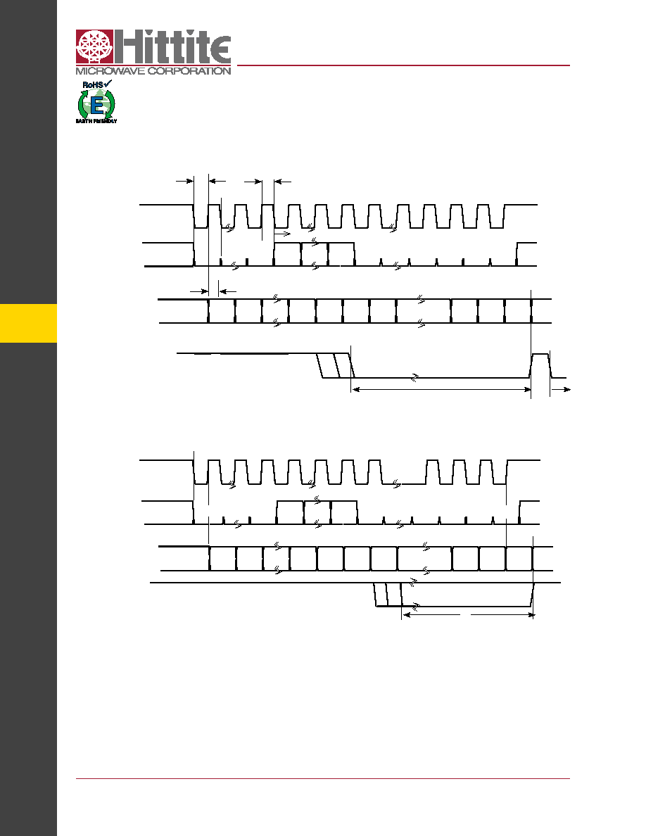
Figure 39. Open Mode - Serial Port Timing Diagram - READ Operation 2-Cycles
sCLK
sDI
sEN
d5
d4
d0
r4
a2
a1
a0
r0
2
19
20
21
24
25
26
31
32
t5
t4
LD_sDO
x
sCLK
2
19
20
21
24
25
26
31
32
30
LD_sDO
Chip Address =000
Register Address =00000
READ Address
LD
sDI
d5
d4
d0
r4
a2
a1
a0
x
r0
d23
x
d30
d10
d9
d8
d7
d6
d2
d1
d0
d3
d31
LD
LD**
x
FIRST CYCLE
SECOND CYCLE
**Note: Read-back on LD_sDO can function without sEN, however sEN
rising edge is required to return the LD_sDO to the LD state
sEN
t3
30
29
发布紧急采购,3分钟左右您将得到回复。
相关PDF资料
HMC830LP6GE
IC FRACT-N PLL W/VCO 40QFN
HMP8117CNZ
IC VIDEO DECODER NTSC/PAL 80PQFP
HMP8156ACNZ
IC VIDEO ENCODER NTSC/PAL 64MQFP
HSP45102SC-40Z
IC OSC NCO 40MHZ 28-SOIC
HSP45106JC-33Z
IC OSC NCO 33MHZ 84-PLCC
HSP45116AVC-52Z
IC OSC NCO 52MHZ 160-MQFP
ICL7109EPL+
IC ADC 12BIT 3-ST 40-DIP
ICM7217AIPI
IC OSC UP/DWN CNTR 2MHZ 28-DIP
相关代理商/技术参数
HMC704LP4ETR
制造商:Hittite Microwave Corp 功能描述:IC FRACT-N PLL 16BIT 24QFN
HMC705LP4
制造商:HITTITE 制造商全称:Hittite Microwave Corporation 功能描述:6.5 GHz PROGRAMMABLE DIVIDER (N = 1 - 17)
HMC705LP4E
制造商:Hittite Microwave Corp 功能描述:IC DIVIDER HBT PROGR 24-QFN
HMC705LP4ETR
功能描述:IC DIVIDER HBT PROGR 24QFN 制造商:analog devices inc. 系列:- 包装:剪切带(CT) 零件状态:在售 功能:分频器 频率:100MHz ~ 6.5GHz RF 类型:- 辅助属性:- 封装/外壳:24-VFQFN 裸露焊盘 供应商器件封装:24-QFN(4x4) 标准包装:1
hmc706lc3c
制造商:Hittite Microwave Corp 功能描述:IC CONV NRZ-RZ 13GBPS 16SMD
HMC707LP5
制造商:HITTITE 制造商全称:Hittite Microwave Corporation 功能描述:0.5 dB LSB 6-BIT DIGITAL VARIABLE GAIN AMPLIFIER, 700 - 1200 MHz
HMC707LP5_10
制造商:HITTITE 制造商全称:Hittite Microwave Corporation 功能描述:0.5 dB LSB 6-BIT DIGITAL VARIABLE GAIN AMPLIFIER, 700 - 1200 MHz
HMC707LP5E
制造商:Hittite Microwave Corp 功能描述:IC AMP DVGA LNA 6-BIT 32-QFN